- 您现在的位置:买卖IC网 > Sheet目录17358 > LM2594APDBCKGEVB (ON Semiconductor)EVAL BOARD FOR LM2594APDBCKG
�� �
�
�LM2594�
�x� t� on�
�[� Load�
�in�
�O�
�in�
�peak�
�2L� 1�
�V�
�O�
�x� 1.0� ,� and� f� osc� +� 52� kHz.�
�fosc�
�where� t� on� +�
�in�
�O�
�across� the� regulator� is� the� absolute� sum� of� the� input� and�
�output� voltages� and� this� must� be� limited� to� a� maximum� of�
�40� V.�
�This� circuit� configuration� is� able� to� deliver� approximately�
�0.25� A� to� the� output� when� the� input� voltage� is� 12� V� or� higher.�
�At� lighter� loads� the� minimum� input� voltage� required� drops�
�to� approximately� 4.7� V,� because� the� buck� ?� boost� regulator�
�topology� can� produce� an� output� voltage� that,� in� its� absolute�
�value,� is� either� greater� or� less� than� the� input� voltage.�
�Since� the� switch� currents� in� this� buck� ?� boost� configuration�
�are� higher� than� in� the� standard� buck� converter� topology,� the�
�available� output� current� is� lower.�
�This� type� of� buck� ?� boost� inverting� regulator� can� also�
�require� a� larger� amount� of� startup� input� current,� even� for�
�light� loads.� This� may� overload� an� input� power� source� with�
�a� current� limit� less� than� 1.0� A.�
�Such� an� amount� of� input� startup� current� is� needed� for� at�
�least� 2.0� ms� or� more.� The� actual� time� depends� on� the� output�
�voltage� and� size� of� the� output� capacitor.�
�Because� of� the� relatively� high� startup� currents� required� by�
�this� inverting� regulator� topology,� the� use� of� a� delayed� startup�
�or� an� undervoltage� lockout� circuit� is� recommended.�
�Using� a� delayed� startup� arrangement,� the� input� capacitor�
�can� charge� up� to� a� higher� voltage� before� the� switch� ?� mode�
�regulator� begins� to� operate.�
�The� high� input� current� needed� for� startup� is� now� partially�
�supplied� by� the� input� capacitor� C� in� .�
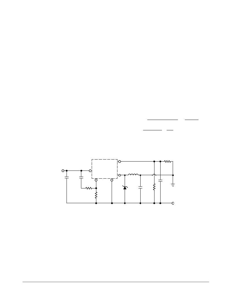
�It� has� been� already� mentioned� above,� that� in� some�
�situations,� the� delayed� startup� or� the� undervoltage� lockout�
�features� could� be� very� useful.� A� delayed� startup� circuit�
�applied� to� a� buck� ?� boost� converter� is� shown� in� Figure� 28.�
�Figure� 30� in� the� “Undervoltage� Lockout”� section� describes�
�an� undervoltage� lockout� feature� for� the� same� converter�
�topology.�
�Design� Recommendations:�
�The� inverting� regulator� operates� in� a� different� manner�
�than� the� buck� converter� and� so� a� different� design� procedure�
�has� to� be� used� to� select� the� inductor� L1� or� the� output�
�capacitor� C� out� .�
�The� output� capacitor� values� must� be� larger� than� what� is�
�normally� required� for� buck� converter� designs.� Low� input�
�voltages� or� high� output� currents� require� a� large� value� output�
�capacitor� (in� the� range� of� thousands� of� m� F).�
�The� recommended� range� of� inductor� values� for� the�
�inverting� converter� design� is� between� 68� m� H� and� 220� m� H.� To�
�select� an� inductor� with� an� appropriate� current� rating,� the�
�inductor� peak� current� has� to� be� calculated.�
�The� following� formula� is� used� to� obtain� the� peak� inductor�
�current:�
�I� (V� )� |V� |)� V�
�I� )�
�in�
�|V� |�
�V� )� |V� |�
�Under� normal� continuous� inductor� current� operating�
�conditions,� the� worst� case� occurs� when� V� in� is� minimal.�
�12� to� 40� V�
�Feedback�
�R4�
�Unregulated�
�DC� Input�
�+V� in�
�LM2594�
�L1�
�100� m� H�
�C� in�
�100� m� F/50� V�
�C1�
�0.1� m� F�
�ON/OFF�
�R2�
�47k�
�GND�
�D1�
�1N5819�
�C� out�
�220� m� F�
�R3�
�C� FF�
�?� 12� V� @� 0.25� A�
�Regulated�
�Output�
�Figure� 24.� Inverting� Buck� ?� Boost� Develops� with� Delayed� Startup�
�http://onsemi.com�
�18�
�发布紧急采购,3分钟左右您将得到回复。
相关PDF资料
EEM15DTBN
CONN EDGECARD 30POS R/A .156 SLD
SJP7401-5/8-50-BLACK
LOOP BLACK 5/8" X 50YD X 0.11"
EEM15DTBH
CONN EDGECARD 30POS R/A .156 SLD
RE-1515S/H
CONV DC/DC 1W 15VIN 15VOUT
GSC05DRTH-S13
CONN EDGECARD 10POS .100 EXTEND
TAAD157M016G
CAP TANT 150UF 16V 20% AXIAL
EEM15DTBD
CONN EDGECARD 30POS R/A .156 SLD
TAAD157M010G
CAP TANT 150UF 10V 20% AXIAL
相关代理商/技术参数
LM2594ASCBCKGEVB
功能描述:BOARD EVAL FOR LM2594ADJ 8-SOIC RoHS:是 类别:编程器,开发系统 >> 评估板 - DC/DC 与 AC/DC(离线)SMPS 系列:* 产品培训模块:Obsolescence Mitigation Program 标准包装:1 系列:True Shutdown™ 主要目的:DC/DC,步升 输出及类型:1,非隔离 功率 - 输出:- 输出电压:- 电流 - 输出:1A 输入电压:2.5 V ~ 5.5 V 稳压器拓扑结构:升压 频率 - 开关:3MHz 板类型:完全填充 已供物品:板 已用 IC / 零件:MAX8969
LM2594DADJG
功能描述:直流/直流开关调节器 0.5A BUCK SW REG 150KHZ RoHS:否 制造商:International Rectifier 最大输入电压:21 V 开关频率:1.5 MHz 输出电压:0.5 V to 0.86 V 输出电流:4 A 输出端数量: 最大工作温度: 安装风格:SMD/SMT 封装 / 箱体:PQFN 4 x 5
LM2594DADJR2G
功能描述:直流/直流开关调节器 0.5A BUCK SW REG 150KHZ RoHS:否 制造商:International Rectifier 最大输入电压:21 V 开关频率:1.5 MHz 输出电压:0.5 V to 0.86 V 输出电流:4 A 输出端数量: 最大工作温度: 安装风格:SMD/SMT 封装 / 箱体:PQFN 4 x 5
LM2594HVM-12
功能描述:直流/直流开关转换器 RoHS:否 制造商:STMicroelectronics 最大输入电压:4.5 V 开关频率:1.5 MHz 输出电压:4.6 V 输出电流:250 mA 输出端数量:2 最大工作温度:+ 85 C 安装风格:SMD/SMT
LM2594HVM-12/NOPB
功能描述:直流/直流开关转换器 150KHZ 0.5A STEP- DOWN VLTG REG RoHS:否 制造商:STMicroelectronics 最大输入电压:4.5 V 开关频率:1.5 MHz 输出电压:4.6 V 输出电流:250 mA 输出端数量:2 最大工作温度:+ 85 C 安装风格:SMD/SMT
LM2594HVM-12/NOPB
制造商:Texas Instruments 功能描述:DC/DC Converter (DC-DC) / Switching Regu
LM2594HVM-3.3
功能描述:直流/直流开关转换器 RoHS:否 制造商:STMicroelectronics 最大输入电压:4.5 V 开关频率:1.5 MHz 输出电压:4.6 V 输出电流:250 mA 输出端数量:2 最大工作温度:+ 85 C 安装风格:SMD/SMT
LM2594HVM-3.3/NOPB
功能描述:直流/直流开关转换器 150KHZ 0.5A STEP- DOWN VLTG REG RoHS:否 制造商:STMicroelectronics 最大输入电压:4.5 V 开关频率:1.5 MHz 输出电压:4.6 V 输出电流:250 mA 输出端数量:2 最大工作温度:+ 85 C 安装风格:SMD/SMT